Making the receiver circuit
The receiver circuit will eventually reside in
Sam’s body, taking the signals that your remote control unit
sends telling Sam how to behave. Here are the steps to build the
receiver circuit:
1. Take two 830-contact breadboards and join
them by inserting the tabs into the slots along the sides to
make one large breadboard.
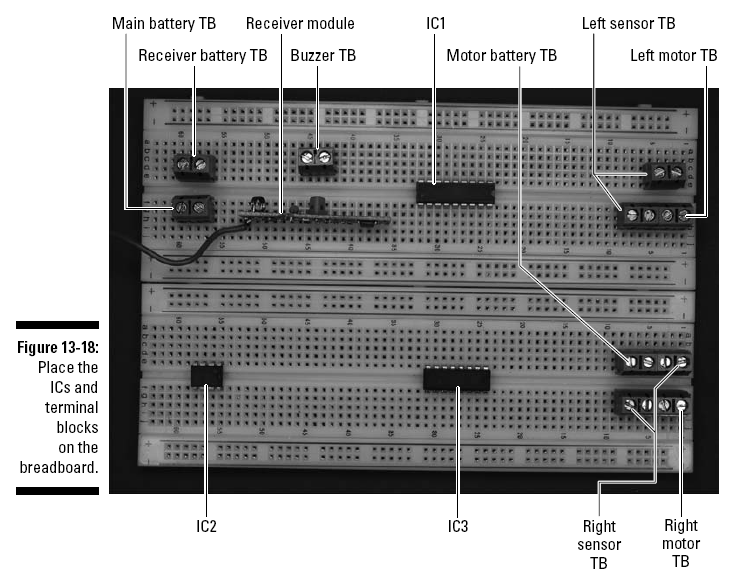
2. Place the HT12D (IC1), the LM555 (IC2), the
L293D (IC3), the receiver module, and ten terminal blocks on the
breadboard, as shown in Figure 13-18.
3. Place the four RB5-5-S relays (Relay 1–Relay
4) and five 2N3904 (Q1–Q5) transistors on the breadboard, as
shown in Figure 13-19.
Insert each transistor lead into a separate
breadboard row with the
• Collector lead to the left side, as shown in
Figure 13-19
• Base lead in the center
• Emitter lead to the right
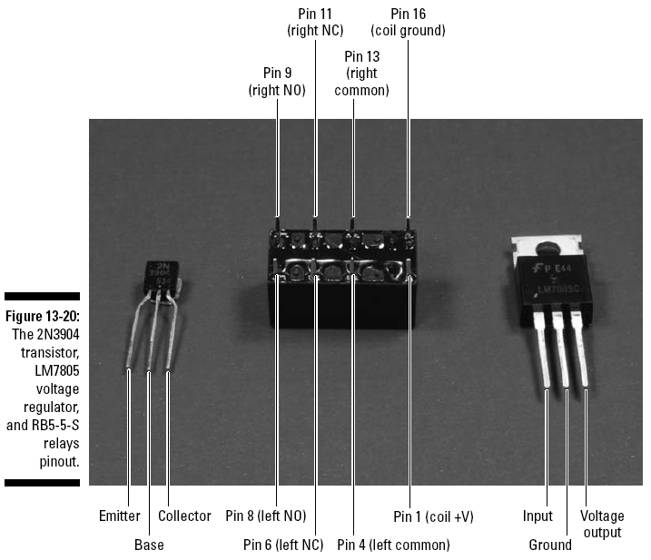
The collector pin of Q2 goes in the same
breadboard row as Pin 16 of Relay 1. The collector pin of Q3
goes in the same breadboard row as Pin 16 of Relay 2. The pin
designations of the 2N3904 transistors and the LM7805 voltage
regulator are shown in Figure 13-20.

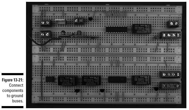
4. Insert wires to connect the ICs, voltage
regulator, transistors, relays, and terminal blocks to the
ground bus. Then insert wires between the ground buses to
connect them, as shown in Figure 13-21.
The ground buses are designated by a negative
(–) sign on this breadboard. Thirty-one shorter wires connect
components to ground bus; the two long and one short wires on
the left connect the ground buses.
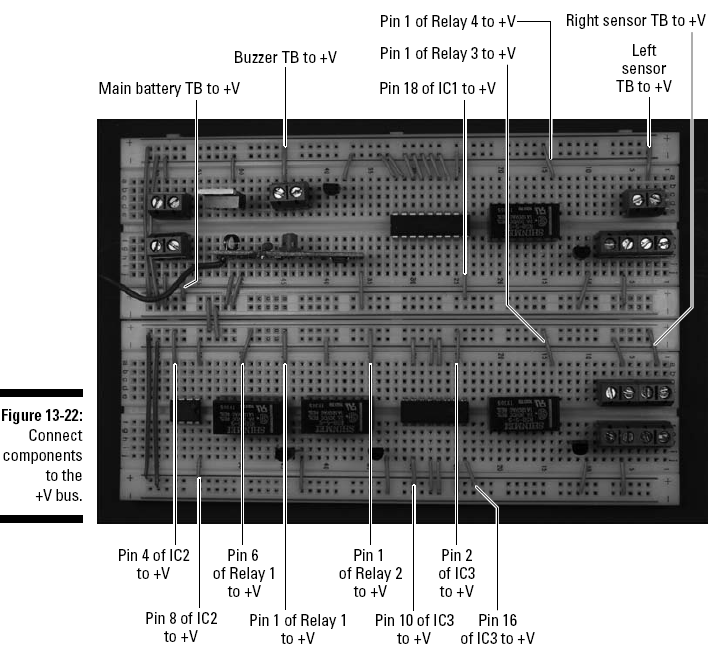
5. Insert wires to connect the ICs, the terminal
blocks, relays, and the voltage regulator to the +V bus. Then
insert wires between the +V buses to connect them, as shown in
Figure 13-22.
The +V buses are designated by a + sign on this
breadboard.
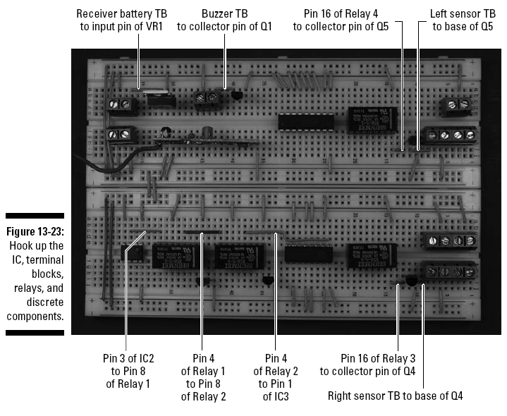
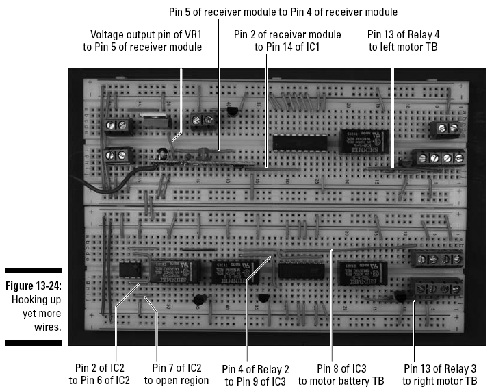
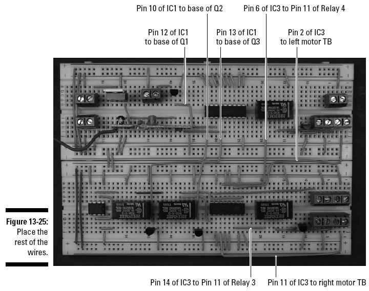
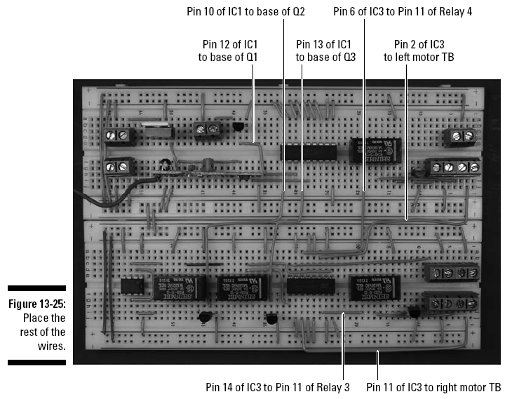
6. Insert wires to connect the ICs, terminal
blocks, relays, and discrete components, as shown in Figures
13-23, 13-24, and 13-25.
The receiver module pinout is shown in Figure
13-26.
7. Insert the following, as shown in Figure
13-27:
• Six 0.1 microfarad ceramic capacitors (C1, C3,
C6, C7, C9, C11)
• Six 10 microfarad electrolytic capacitors (C2,
C4, C5, C8, C10, C12)
• 51 kohm resistor (R1)
• Three 10 kohm resistors (R3, R5, R7)
• Two 150 ohm resistors (R4, R6)
• 330 ohm resistor (R2)
Use both the schematic and the photo to help you
place each component.
For example, the schematic shows that the + side
of C5 is connected to Pin 2 of IC2 and the other side of C2 is
connected to ground, so insert the long lead of C2 in the same
row as Pin 2 of IC2 and the short lead in the ground bus.
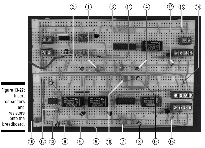
Use the following key for the callouts in Figure
13-27.
1. C1 from +V bus to ground bus
2. C2 from +V bus to ground bus
3. C3 from +V bus to ground bus
4. C4 from +V bus to ground bus
5. C7 from +V bus to ground bus
6. C8 from +V bus to ground bus
7. C9 from +V bus to ground bus
8. C10 from +V bus to ground bus
9. C5 from Pin 2 of IC2 to ground bus
10. C6 from Pin 5 of IC2 to ground bus
11. R1 from Pin 15 of IC1 to Pin 16 of IC1
12. R2 from Pin 6 of IC2 to Pin 7 of IC2
13. R3 from Pin 7 of IC2 to +V
14. R4 from right sensor TB to ground
15. R6 from left sensor TB to ground
16. R5 from right sensor TB to +V
17. R7 from left sensor TB to +V
18. C11 from +V bus to ground bus
19. C12 from +V bus to ground bus